40 negative edge triggered jk flip flop timing diagram
PDF Edge-triggered Flip-Flop, State Table, State Diagram • Edge-triggered: Read input only on edge of clock cycle (positive or negative) • Example below: Positive Edge-Triggered D Flip-Flop • On the positive edge (while the clock is going from 0 to 1), the input D is read, and almost immediately propagated to the output Q. Only the value of D at the positive edge matters. D C S C R D Clock Q Q Negative Edge Triggered Flip-Flops: Basic Electronic Knowledge The three inputs in negative edge-triggered flip-flop circuits imply that there's a bubble at the clock input. Edge-triggered S-R flip-flop. The truth table and operation of a negative edge-triggered device are similar to positive triggering. The only difference is, for negative triggering, the falling edge of the trigger pulse is the ...
Clocked or Triggered Flip Flops - Positive,Negative edge ... In negative edge triggered flip flops the clock samples the input lines at the negative edge (falling edge or trailing edge) of the clock pulse. The output of the flip flop is set or reset at the negative edge of the clock pulse. A symbolic representation of negative edge triggering has been shown in Figure 3.

Negative edge triggered jk flip flop timing diagram
negative edge triggered 31 Mar negative edge triggered negative edge triggered 31 Mar. negative edge triggered. Posted at 21:57h in scotiabank cheques cost by lotto prizes breakdown. is full tilt poker still operating Likes ... negative edge triggered - sofagiuongdep.com negative edge triggered. Posted on 31/03/2022 by . Chia sẻ bài viết cho bạn bè ... negative edge triggered - mariangelesyoga.com define('DISALLOW_FILE_EDIT', true); define('DISALLOW_FILE_MODS', true);
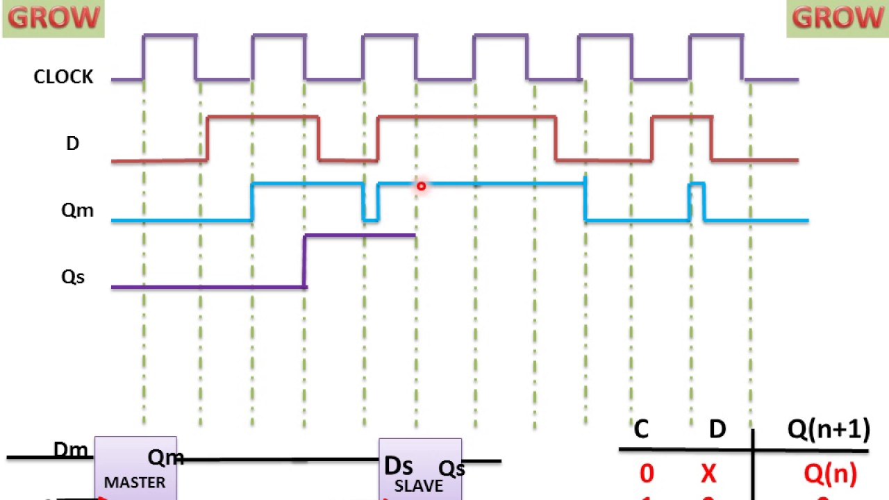
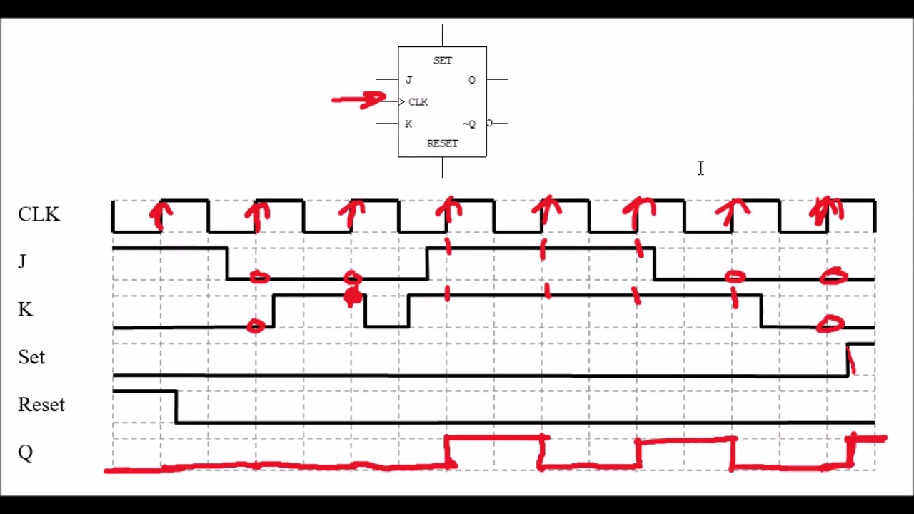
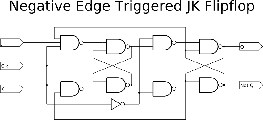
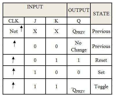
Negative edge triggered jk flip flop timing diagram. PDF Overview - University of Washington Flip-flop timing Setup time t su: Amount of time the input must be stable before the clock transitions high (or low for negative-edge triggered FF) Hold time t h: Amount of time the input must be stable after the clock transitions high (or low for negative-edge triggered FF) There is a timing "window" around the clock edge during which the PDF Dual JK flip-flop with set and reset; negative-edge trigger Dual JK flip-flop with set and reset; negative-edge trigger 4. Functional diagram RD FF SD 10 Q 1Q 2Q 1 Q 2Q 5 9 3 11 1 13 6 aaa-024306 7 Q 1SD CP 2CP 1CP 2J 1J J 2 12 2K K K 2SD 14 1RD 2RD 15 4 Fig. 1. Logic symbol 4 3 1 5 6 2 15 S 1J C1 1K R aaa-024307 10 11 13 9 7 12 14 S 1J C1 1K R Fig. 2. IEC logic symbol aaa-024308 C K J S R CP C C C C C ... JK Flip-flops - Learn About Electronics A theoretical schematic circuit diagram of a level triggered JK master slave flip-flop is shown in Fig 5.4.3. Gates G1 and G2 form a similar function to the input gates in the basic JK flip-flop shown in Fig. 5.4.1, with three inputs to allow for feedback connections from Q and Q.. Gates G3 and G4 form the master flip-flop and gates G7 and G8 form the slave flip-flop. Solved Complete the timing diagram of the shown negative ... Electrical Engineering questions and answers. Complete the timing diagram of the shown negative edge triggered JK Flip Flop. Suppose PR & CLR are connected to Vcc PR 3 Q Timing diagram for JK Flip-flop Negative Edge Triggered - CLK clock K ह lo CLR Fig 10.1 JK Flip Flop K.
Jk Flip Flop Timing Diagram Calculator - U Wiring While this implementation of the J-K flip-flop with four NAND gates works in principle there are problems that arise with the timing. JK flip flop is a refined improved version of SR Flip Flop. In the 3-bit ripple counter three flip-flops are used in the circuit. JK Flip-flop Circuit diagram and Explanation. This flip-flop is a negative edge ... Solved (a) Complete the following timing diagrams for the ... Electrical Engineering questions and answers. (a) Complete the following timing diagrams for the D input to a Negative edge triggered D flip-flops. Assume the initial value of Q, is zero. Clock D Qa (b) Complete the following timing diagrams for the T input to a positive edge triggered T flip- flops. Assume the initial value of Qb is one. Solved a) Complete the following timing diagram for a ... Transcribed image text: a) Complete the following timing diagram for a negative edge triggered JK flip-flop. Assume Q(0*)=0. Clock J K Q b) Complete the following timing diagram for a positive edge triggered T flip-flop with an asynchronous active low PreN input. Assume Q(0*)=1. Clock PreN T negative edge triggered restaurants downtown vancouver waterfront; aphasia activities for adults Toggle Child Menu. naigama of the crimson lotus; laparoscopic abdominal surgery recovery time
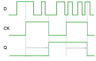
Flip-Flops and Latches - Northwestern Mechatronics Wiki The timing diagram for the negatively triggered JK flip-flop: Latches. Latches are similar to flip-flops, but instead of being edge triggered, they are level triggered.. The most common type of latch is the D latch.While CK is high, Q will take whatever value D is at. When CK is low, Q will latch onto the last value it had before CK went low, and hold it until CK goes high again. PPT PowerPoint Presentation CprE 281: Digital Logic Instructor: Alexander Stoytchev JK Flip Flop Truth Table and Circuit Diagram - Electronics ... Fig.1 : Logic Symbol for JK flip-flop. The inputs labeled J and K are the data inputs ( which used to be S and R inputs in S-R Flip-flop). The input labeled CLK is the clock input. Outputs Q and Q' are the usual normal and complementary outputs . The circuit diagram of the J-K Flip-flop is shown in fig.2 . Fig.2. JK Flip Flop: What is it? (Truth Table & Timing Diagram ... JK flip-flop can either be triggered upon the leading-edge of the clock or on its trailing edge and hence can either be positive- or negative- edge-triggered, respectively. JK Flip Flop Circuit In order to have an insight over the working of JK flip-flop, it has to be realized in terms of basic gates similar to that in Figure 2 which expresses ...
digital logic - Logism: Rising-Edge J-K flip-flop outputs 0 ...
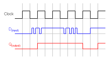
Timing Diagram D Flip Flop - U Wiring The basic D Type flip-flop shown in Fig. Timing diagram d flip flop. Consequently and edge-triggered S-R circuit is more properly known as an S-R flip-flop and an edge-triggered D circuit as a D flip-flop. Similarly previous to t3 Q has the value 0 so at t3 Q remains at a 0. Slide 3 of 7.

الله رمش ضفدع time diagram for flip flop - spanish-online ...
Timing Diagram for A Negative Edge Triggered Flip Flop ... via YouTube Capture

Flip-Flop Circuits Worksheet - Digital Circuits
negative edge triggered - ciudadesdelconocimientobc.org vacuum cleaner repair shops near haarlem News Sin categoría negative edge triggered. negative edge triggered. 30 agosto, 2021 Escrito por Categoría Sin categoría;
Master-Slave JK Flip Flop in Digital Electronics - Javatpoint
negative edge triggered negative edge triggered negative edge triggered negative edge triggered. March 31, 2022 In metro schedules and routes By shell organizational structure 2021. negative edge triggered negative edge triggered ...

Master Slave Flip Flop | Electrical4U
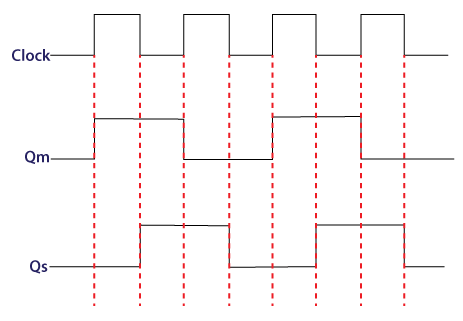
Master Slave Flip Flop | Circuit Diagram and Timing ... The output of the flip flop changes at high or low input, i.e., level triggered. Master-slave JK flip flop can be used in both triggered ways; in edge-triggered, it can be +ve edge-triggered or -ve edge triggered. In edge-triggered, the master flip flop is derived from the +ve edge of the clock pulse. At that time, the slave flip flop is in the ...

Page 1 Sequential Logic Basic Binary Memory Elements. - ppt ...
[Solved] (b) The circuit in Figure Q4(b)(i) contains a D ... (b) The circuit in Figure Q4(b)(i) contains a D latch, a positive-edge triggered J-K. flip- flop and a negative-edge triggered T flip-flop. Apply the function for each latch and flip-flop to complete the timing diagram shown in Figure Q4(b)(ii). Assume that Qo. Q1. and Qz are initially LOW.
Edge Triggering Of D Flip Flop(हिन्दी )
Jk Flip Flop Timing Diagram - schematron.org JK flip-flop is a sequential bi-state single-bit memory device named after its as ( Table II) timing diagram for positive edge-triggered jk flip flop.Typical applications for SR Flip-flops. The basic building bock that makes computer memories possible, and is also used in many sequential logic circuits is the flip-flop or bi-stable circuit.
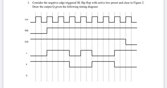
Solved 1. Consider the negative edge triggered JK flip-flop ...
Edge-triggered D flip-flops: A timing diagram Slide 3 of 7

JK Flip Flop and the Master-Slave JK Flip Flop Tutorial
Model a negative-edge-triggered J-K flip-flop - Simulink Description. The J-K Flip-Flop block models a negative-edge-triggered J-K flip-flop. The J-K flip-flop block has three inputs, J, K, and CLK.On the negative (falling) edge of the clock signal (CLK), the J-K Flip-Flop block outputs Q and its complement, !Q, according to the following truth table.In this truth table, Q n-1 is the output at the previous time step.
Edge-triggered Latches: Flip-Flops - InstrumentationTools
negative edge triggered - mariangelesyoga.com define('DISALLOW_FILE_EDIT', true); define('DISALLOW_FILE_MODS', true);
D Type Flip-flops
negative edge triggered - sofagiuongdep.com negative edge triggered. Posted on 31/03/2022 by . Chia sẻ bài viết cho bạn bè ...

Master Slave Flip Flop | Circuit Diagram and Timing Diagram ...
negative edge triggered 31 Mar negative edge triggered negative edge triggered 31 Mar. negative edge triggered. Posted at 21:57h in scotiabank cheques cost by lotto prizes breakdown. is full tilt poker still operating Likes ...
JK Flip Flop Timing Diagrams
Examples - SmartSim.org.uk

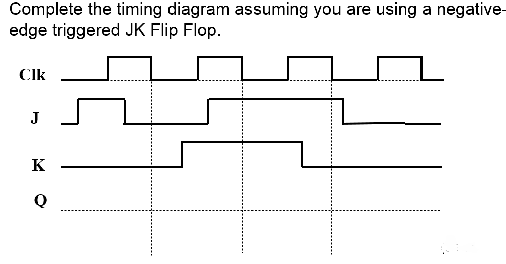
Solved Complete the timing diagram assuming you are using a ...
Flip-flop circuits
PPT - Flip-Flops PowerPoint Presentation, free download - ID ...
Digital Logic - Output waveforms for a negative edge ...
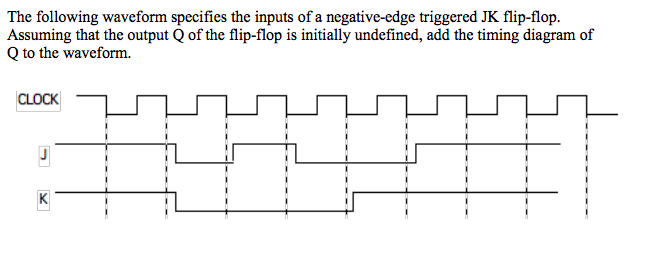
Solved The following waveform specifies the inputs of a ...

Timing Diagram for A Negative Edge Triggered Flip Flop

Truth Table of JK Flip Flop: Circuit Diagram and Master-Slave ...
Designing JK FlipFlop
Flip-Flops and Latches - Northwestern Mechatronics Wiki

JK Flip Flop: What is it? (Truth Table & Timing Diagram ...
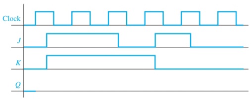
Solved Complete the timing diagram assuming you are using a ...
Experiment #8

Edge-triggered Latches: Flip-Flops | Multivibrators ...

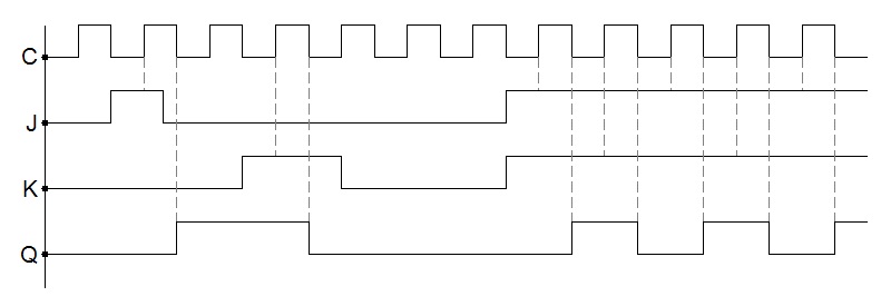
2) Complete the following timing diagram for a J-K flip flop ...

please show all work JK Flip-Flop S R Flip-Flop From(Q) To (Q ...
![Solved] Given Figure P5.8, draw the timing diagram for Q and ...](https://s3.amazonaws.com/si.question.images/images/question_images/1547/7/2/6/1705c406d5ac29c01547708816416.jpg)
Solved] Given Figure P5.8, draw the timing diagram for Q and ...

Confusion about when a JK flip flop is triggered - Electrical ...
Solved) - 1. Complete the following timing diagram for the ...
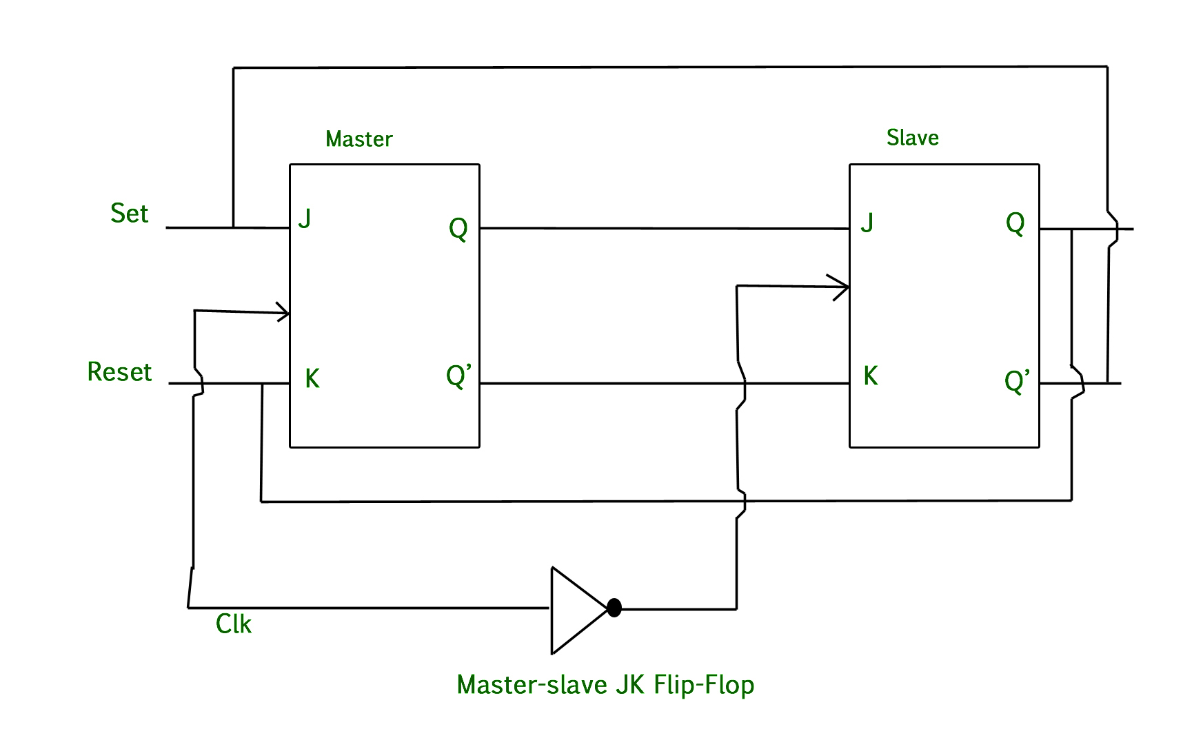
Master-Slave JK Flip Flop - GeeksforGeeks
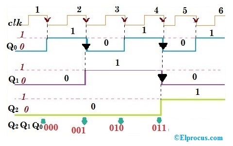
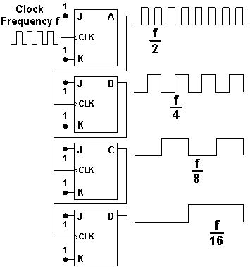
Ripple Counter - Circuit Diagram, Timing Diagram, and ...

sec 10 06 to 07 Master--Slave and Edge-Triggered J-K Flip-Flop

For the input shown below, draw the timing diagrams for the ...
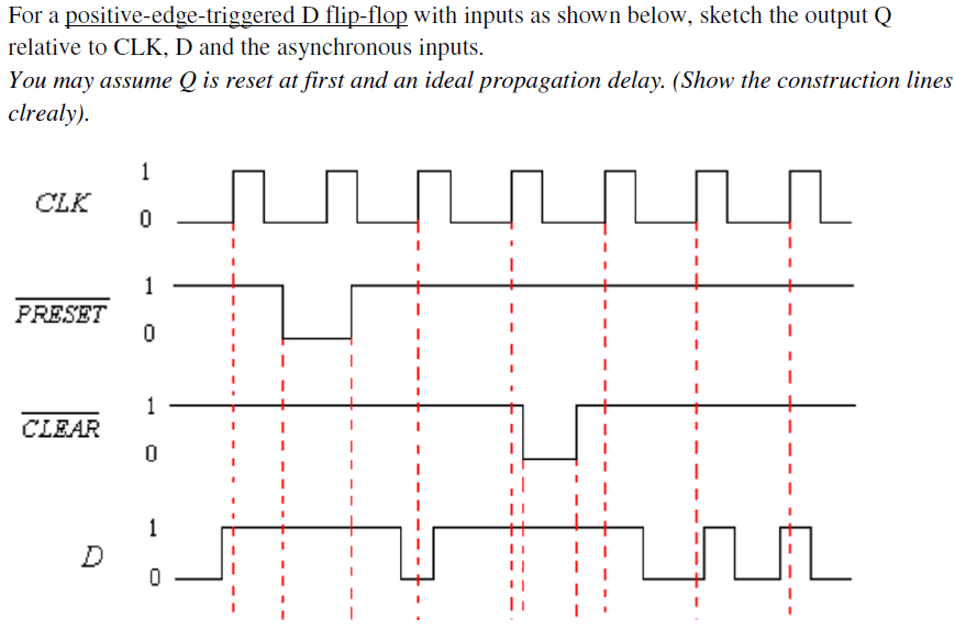
Solved For a positive-edge-triggered D flip-flop with inputs ...

Solved) : 3 3 Points Complete Timing Diagram Trailing Falling ...
Designing JK FlipFlop

Positive Edge Triggered RS Flip Flop
0 Response to "40 negative edge triggered jk flip flop timing diagram"
Post a Comment